Recently, Yu Weili of the Photonics Laboratory of Changchun Institute of Optics, Fine Mechanics and Physics, Chinese Academy of Sciences and Guo Chunlei, a research team from the University of Rochester, collaborated on the performance of photodetectors based on perovskite polycrystalline thin films that are vulnerable to grain boundaries and grain defects Affecting the problem, the MAPbBr3 thin single crystal with extremely low surface defect density was synthesized by the space-limited inverse temperature crystallization method, and the high-quality thin single crystal was combined with a single layer of graphene with high carrier mobility to prepare An efficient vertical structure photodetector has been developed.
In recent decades, photodetectors have received extensive attention from academia and industry, and have been widely used in optical communications, environmental monitoring, biological detection, image sensing, space detection and other fields. Methylammonium halide lead perovskite (CH3NH3PbX3, X=Cl, Br, I) is a perovskite material that has emerged in recent years because of its direct band gap, wide spectral response, high absorption coefficient, and high carrier The advantages of mobility and long carrier diffusion coefficient have gradually become the frontier hot materials for the preparation of photodetectors. At present, the performance of photodetectors based on perovskite polycrystalline thin films is still at a certain distance from expectations. One of the main reasons is that the transmission of carriers at the interface is easily affected by grain boundaries and grain defects. Many research groups have attempted to combine perovskite polycrystalline thin films with high-mobility two-dimensional materials to improve device performance and have achieved certain results, but the negative effects of perovskite polycrystalline grain boundaries have not been resolved.
The MAPbBr3 thin single crystal grown by the space-limited inverse temperature crystallization method has sub-nanometer surface roughness and no obvious grain boundaries. It can combine high-quality perovskite single crystal synthesis technology and single-layer graphene transfer Technology to prepare high-performance vertical structure photodetectors. The prepared vertical structure photodetector has a high photodetection rate at room temperature (~2.02×10¹³ Jones); compared with the photodetector of pure perovskite MAPbBr3 single crystal film under 532nm laser irradiation, the perovskite The photoelectric performance (photoresponse, photodetection rate and photoconductive gain) of the mine-graphene composite vertical structure photodetector has been improved by nearly an order of magnitude. Carrier ultrafast kinetics studies have shown that the improved performance of the device is mainly due to the increased lifetime of perovskite carriers of high-quality perovskite single crystals and the effective extraction and transport of free charge by graphene. Related results have been published in Small (DOI: 10.1002/smll.202000733).
The study effectively combined the perovskite single crystal material and the two-dimensional material graphene. Using the synergistic advantages of the two in carrier generation and transportation, the device performance was improved, and the device structure and energy band were demonstrated. The design's ability to control the performance of the device provides new ideas for the preparation of high-performance perovskite photodetectors.
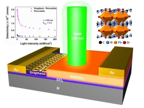
High sensitivity perovskite single crystal-graphene composite vertical structure photodetector
200 Series Sheets,201 Stainless Sheet,Stainless Sheet Price,Stainless Steel Flat Sheet
Foshan Sunsteel Co. , Ltd , https://www.fssunsteel.com